| Home Page |
| Examples |
| Products |
| Support |
|
Examples of using TEM Substrates |
|
Noble metal substrates are sufficiently conducting for electroplating and electrochemistry studies. Here a 2-nm platinum film was used to demonstrate copper plating. Related article: Daniel B. Allred, Melvin T. Zin, Hong Ma, Mehmet Sarikaya, François Baneyx, Alex K.-Y. Jen, Daniel T. Schwartz, "Direct nanofabrication and transmission electron microscopy on a suite of easy-to-prepare ultrathin film substrates", Thin Solid Films, 515 (13): 5341 - 5347, 2007. |
|
|
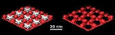
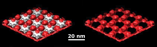
With tomography, three-dimensional structure can be obtained. Therefore cross-sections can be taken without cross-sectioning. Related article: Daniel B. Allred, Anchi Cheng, Mehmet Sarikaya, François Baneyx, Daniel T. Schwartz, "Three-dimensional architecture of inorganic nanoarrays electrodeposited through a surface-layer protein mask", Nano Letters, 8 (5): 1434 - 1438, 2008. |
|
|
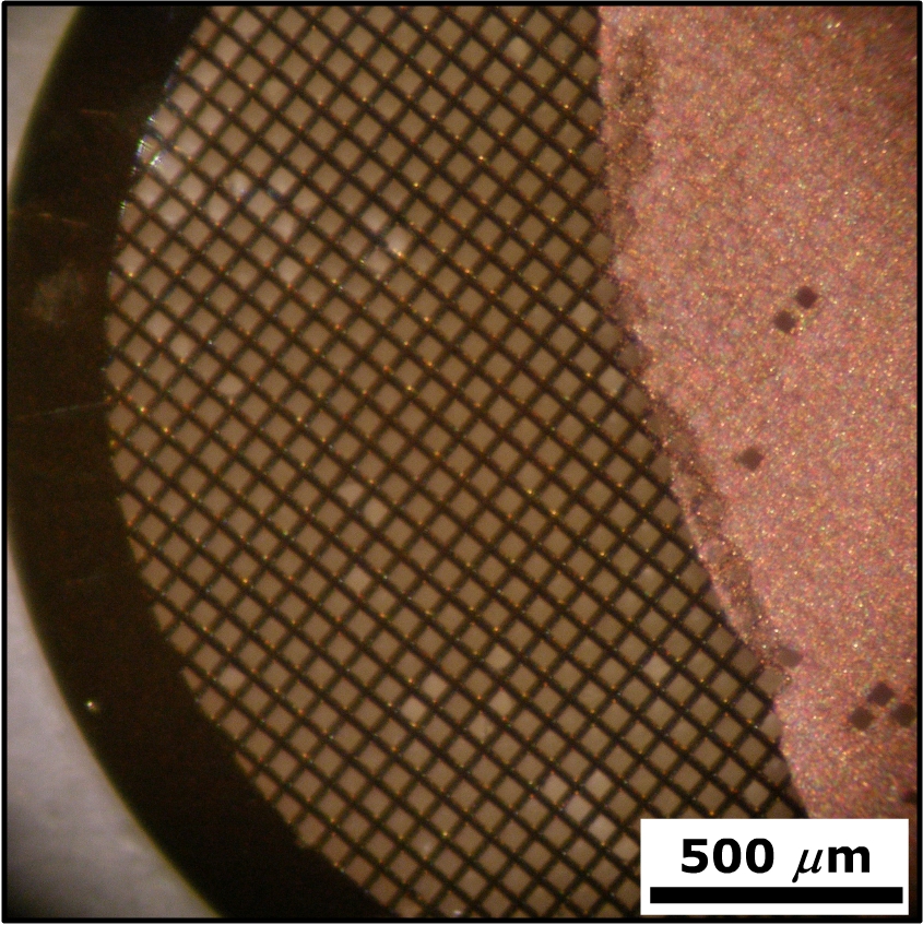
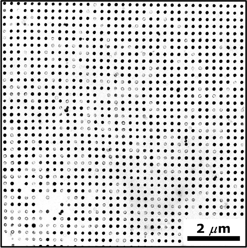
Surprisingly, thin gold / platinum films survived the microcontact printing process. This allows investigation of surface functionalization in a way not performed traditionally. Related article: Daniel B. Allred, Melvin T. Zin, Hong Ma, Mehmet Sarikaya, François Baneyx, Alex K.-Y. Jen, Daniel T. Schwartz, "Direct nanofabrication and transmission electron microscopy on a suite of easy-to-prepare ultrathin film substrates", Thin Solid Films, 515 (13): 5341 - 5347, 2007. |
|
|
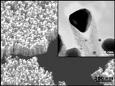
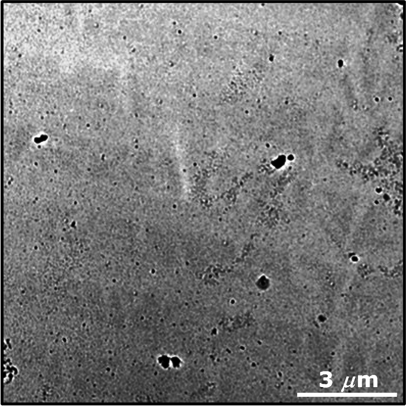
Choice of substrates can influence catalytic reactions, such as the use of platinum in iron-catalyzed formation of carbon nanofibers here. Unpublished data, for related article on carbon nanofibers: Yusuke Ominami, Quoc Ngo, Makoto Suzuki, Alexander J. Austin, Cary Y. Yang, Alan M. Cassell, Jun Li, "Interface characteristics of vertically aligned carbon nanofibers for interconnect applications", Applied Physics Letters, 89 : 263114 (1 - 3), 2006. |
|
|
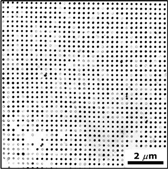
The thin films can withstand the process of spin-coating, making them suitable substrates for studying lithography processes. Related article: Daniel B. Allred, Melvin T. Zin, Hong Ma, Mehmet Sarikaya, François Baneyx, Alex K.-Y. Jen, Daniel T. Schwartz, "Direct nanofabrication and transmission electron microscopy on a suite of easy-to-prepare ultrathin film substrates", Thin Solid Films, 515 (13): 5341 - 5347, 2007. |

|
*Copyright© 2006, University of Washington, used with permission |


